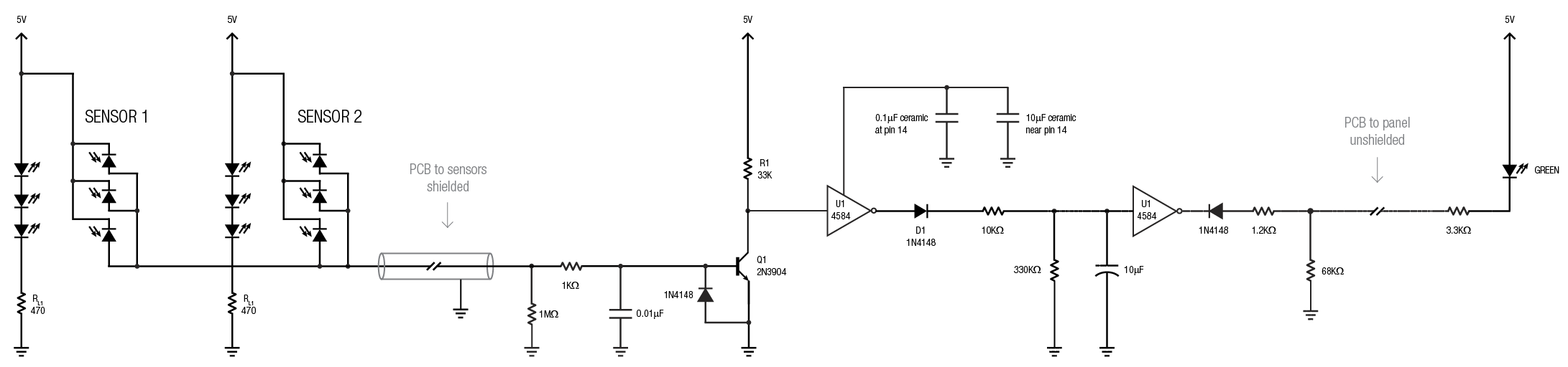
After a couple weeks pointing and clicking I have a detector circuit board design complete. It has a finished size of 2-5/8″ x 10-3/4″ and contains 10 detector circuits each with two sensor inputs. To save you from flipping back a bunch of posts, here is the schematic for a single detector circuit…
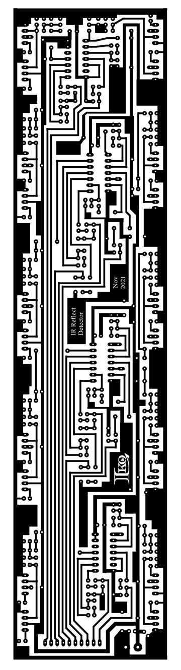
Tall slender boards were called for because they will mount on the helix uprights. My inkjet transparencies are 8-1/2″ x 11″ minus an unprintable margin on all sides. Some quickie pencil sketches and back-of-envelope measurements indicated I should be able to get three boards on a transparency allowing for two 1/16″ cut lines and 1/4″ horizontal margins.
8-1/2″ – 1/4″ – 1/4″ = 8″ (margins)
8″ – 1/16″ – 1/16″ = 7-7/8″ (cuts)
7-7/8″ / 3 = 2.625″
The vertical dimension uses the full vertical printing area of the transparency minus 1/8″ margins.
Here is what I ended up with:
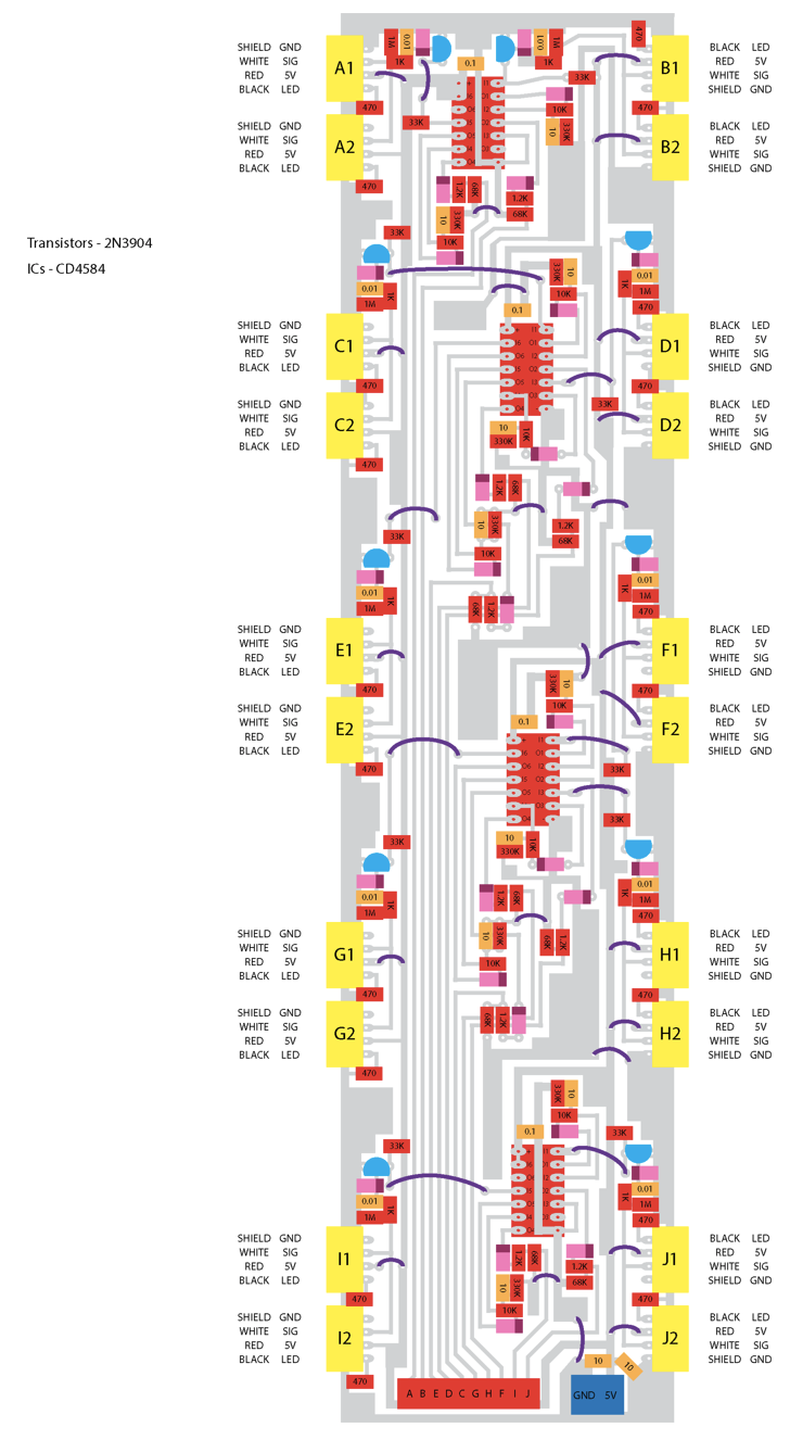
A board this size would really benefit from the use of surface mount devices because of their small footprint. My electronics parts inventory is almost exclusively through-hole devices. I can’t rationalize buying all new components when I have drawers full of through-hole parts. So, I am reviving an old school method used many years ago in transistor radios – stand them up. This gives through-hole a footprint closer in size to surface mount.

I know there are software packages available that make circuit and board design much, much easier than the way I do it with Illustrator. But since I make a circuit board maybe only once every five years and never send them out for production it isn’t worth my time to learn new software. Especially since I know Illustrator like the back of my hand and am pretty quick with it.
IC pin spacing is 0.100″ (2.54mm). So, I begin with a 0.100″ grid allowing 0.200″ for my stand up components. From there it is more trial and err than anything else. Keep moving things around and rerouting traces on the grid until everything fits and is connected together according to the schematic. I started with the 10 pin signal connector and 2 pin power connector at the bottom and worked my way up using scale sized component representations. During the design process I made the 5V supply rail brown and the ground plane green to make things easier. Because the board is 10 copies of the same circuit, in many cases I could design a particular part of the circuit once and then clone it over and over.
Resistors are red
Capacitors are orange
Diodes are burgundy
Transistors are light blue
Jumpers are violet
IC sockets and signal out connector are red
Power connector is dark blue
Sensor connectors are yellow

Finally, I made a placement drawing as a guide to use when soldering the components in place. I’ll print this on big 11×17 paper so it easy to read the component values.
Time to setup the workbench for circuit board production. Back soon.

As always, a superbly professional undertaking, with entirely professional results. Impressive indeed.
Thanks Dwight.
Wow. I have zero aptitude for this type of technology so it boggles my mind when I see something of this nature. Incredibly impressive. You have proven once again just how diverse the hobby can be.
Seriously I’d spend a week just looking at, and admiring your electronics work & wiring…!
It’s an art form within a hobby…
Looking forward to seeing it operational.